Technology portfolio for quantum and neuromorphic computing

slide 1
slide 1
slide 1
slide 1
slide 1
slide 1
slide 1
slide 1
slide 1
slide 1
slide 1
slide 1
slide 1
slide 1
slide 1
slide 1
slide 1
slide 1
slide 1
slide 1
slide 1
slide 1
slide 1
slide 1
slide 1
slide 1
slide 1
slide 1
slide 1
slide 1
slide 1
slide 1
slide 1
slide 1
slide 1
slide 1
slide 1
slide 1
slide 1
slide 1
slide 1
slide 1
slide 1
slide 1
slide 1
slide 1
slide 1
slide 1
slide 1
slide 1
slide 1
slide 1
slide 1
slide 1
slide 1
slide 1
slide 1
Ultra-low loss integrated photonic platform based on silicon nitride waveguides
low loss integrated photonic platform based on aluminum nitride
AlGaN Photonic Integrated Circuit for fast light switching and routing
Single-pass Lithium-niobate-on-insulator (LNOI) waveguide
LiNbO3 and Si3N4 waveguide circuits for optical qubit I/O
LNOI resonators for efficient nonlinear frequency conversion
AlGaN bragg waveguide for efficient coupling to single photon emitters like defect centers or atoms
Diffractive metasurfaces for flat lenses and precise light shaping in confined configurations
Quantum-grade diamond grown via chemical vapor deposition
Quantum-grade diamond synthesis and doping
Quantum grade SiC epitaxy and generation of color centers
Diamond & silicon carbide nano-fabrication and integration of defect centers (N, Si, Ge, Sn-Vacancies)
Lens structures enhancing light coupling to color centers in SiC
Nitrogen-vacancy centers in quantum-grade diamond
Monolithic ion trap fabricated using Selective Laser-induced Etching (SLE)
Laser polishing to optical quality and laser welding of SLE manufactured glass components
Electro-optical circuit board – integration of optical waveguides and electrical conductors on glass
Back-end-of-line wafer technology for combining photonic integrated circuits with electronic components
Glass-based package for on-chip photonic quantum computing with neutral atoms in UHV
Full value-chain laser diode development based on GaAs & GaN
InP laser diodes, balanced detectors, SPAD diodes and SPAD detectors with high quantum efficiency
Full value-chain laser diode development based on GaAs & GaN
From customized laser diodes to micro integrated light control modules
Manufacturing processes for cryogenic qubit technologies on up to 300 mm wafer technology
Growth of CMOS compatible Si/SiGe quantum heterostructures and their structural characterization (200 mm silicon wafers)
Fabrication of superconducting qubit chips, frontend & 3D heterointegration technologies
Superconducting metal coplanar waveguide resonator
E-beam structured resist for gate architecture of spin qubit shuttle
Etched electrodes architecture for spin qubit shuttle
Precisely controlled suspension of carbon nanotubes or graphene
Wafer-level processing of various metals, insulators, and supercon-ductors, e.g., for ion traps
Flexible, shielded and high density superconducting wiring for qubits
Cryogenic characterization of superconducting materials
Quantum Hall characterization of two-dimensional electron gases (2DEG) at 1.5 Kelvin and 12 Tesla
Microstructural and chemical analysis down to the atomic level with spectroscopic scanning TEM
Thermomechanical optimization for cryogenic packages & components. Design, simulation, test & validation
Multi-channel FPGA-based dynamical control for optical modulators (AOMs and EOMs)
Coherent multi-signal sources for qubit control and readout at cryogenic and room temperature
SiGe chip design chain for cryogenic control and readout electronics
Cryogenic electronics and characterization (4K)
Cryogenic low-noise amplifiers for qubit read-out (50 nm mHEMT)
Customizable and miniaturizable SPAD array detectors with lowest dark count rate and high sensitivity
Silicate and direct bonding for quantum optical components
Micromirror-based spatial light modulators for precise holographic beam shaping
Micromirror array allowing fast modulation of light in phase and intensity with high spatial resolution
Design of MEMS phase shifter for linear optical quantum computing
1D and 2D MEMS scanning mirrors for high laser power or large deflection angles
MEMS wafer-level free-form glass with optical quality, e.g. for vacuum packaging with getter integration
MEMS mirrors in hermetically sealed packages with through glass vias
MEMS device with wafer-level integrated NdFeB micromagnets
Superconducting micro bumps for high density integration
Massive parallel assembly of photonic devices via micro-transfer bonding with precise self-alignment
Broadband electro-magnetic shielding with high optical transmission for neutral atoms
Submicrometer-precise addressing unit for ions utilizing fibre coupled waveguide chip and micro-optics
Design, setup and qualification of laser beam shaping optics for QC
Submicrometer-precise addressing unit for ion trap quantum computer
TE&TM polarization maintaining laser setup, including auxiliary target for active beam (pre-)alignment
previous arrow
next arrow
Shadow

We offer research groups, start-ups, and industrial companies customized solutions in microelectronics, nanoelectronics, and photonics. With state-of-the-art microelectronic systems and comprehensive process expertise, the new FMD-QNC expansion module supports your development of hardware for quantum and neuromorphic computing in Germany and Europe.

FMD-QNC supports a variety of platform technologies, including:

  • Superconducting qubits
  • Solid-state spin qubits
  • Neutral atoms
  • Ion traps
  • Photonic platforms
  • Analog and neuromorphic computing architectures
  • Various memristor technologies
Leistungskatalog: Komponenten, Schaltkreise, ModuleProzesstechnologien, Aufbau, Pilotfertigung Test, Charakterisierung, Validierung Design, Simulation, Architektur

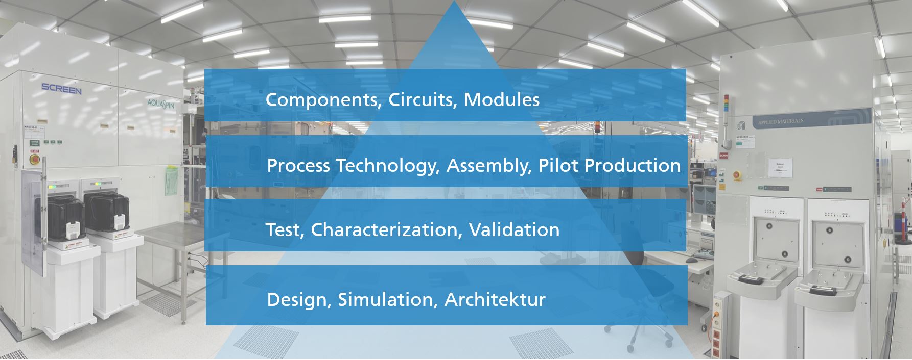
In addition to our research and pilot production capacities, we offer you comprehensive services in design, simulation, system integration, testing and validation. This enables us to provide you with solutions that meet the demanding requirements for scaling your hardware systems and their subsequent transfer to the industry.

Technology offerings by application area (in German)

Enabling technologies for cryogenic platforms:

Enabling technologies for atomic and photonic platforms:

Further enabling technologies for quantum platforms:

Enabling technologies for neuromorphic computing:

Benefit from our networked cleanroom infrastructure and modern machinery, which offers you technological breadth, top quality, and flexibility. Our joint office coordinates all partners to guarantee optimum solutions for your scientific and industrial requirements.

Do not hesitate to contact us to discuss your specific requirements and help us realize your visions for the computing of the future.

Logo Forschungsfabrik Mikroelektronik Deutschland
Logo AMO GmbH Aachen
Logo Jülich Forschungszentrum
Sponsored by the federal ministry of education and research